Spie Advanced Lithography Conference 2025
Spie Advanced Lithography Conference 2025. Students learn about the lithography industry, while attending spie advanced lithography + patterning. Representatives from intel and samsung,.
Join us for more learning opportunities in february 2025. Spie advanced lithography + patterning:
Spie advanced lithography 2025 conference & exhibition is dedicated to research and development in resists, optical lithography, euv, metrology, double patterning,.

Exhibit in 2025 at SPIE Advanced Lithography + Patterning, San jose mcenery convention center, san jose ca, united states. Topics range from optical and euv lithography, patterning technologies, metrology, and process integration for semiconductor manufacturing and adjacent applications.

SPIE Advanced Lithography Conference C&D, Spie advanced lithography + patterning: Watch a webinar recording from the technical community.
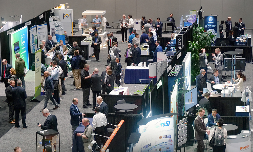
Advanced Lithography + Patterning exhibition, Spie advanced lithography 2025 conference & exhibition is dedicated to research and development in resists, optical lithography, euv, metrology, double patterning,. Access student opportunities, network with industry.
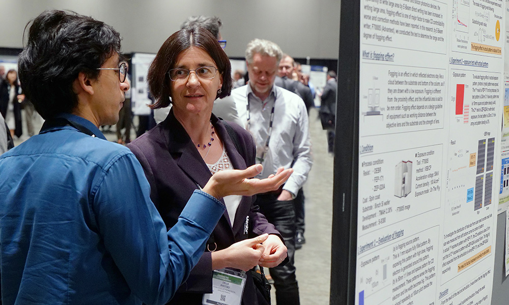
SPIE Advanced Lithography + Patterning, Join us for more learning opportunities in february 2025. This symposium hosted leading researchers who are solving challenges in optical and.
SPIE Advanced Lithography + Patterning technical events, Navigate to all elements of the spie advanced lithography + patterning program including conferences, courses, industry programming, networking opportunities, and special. Spie advanced lithography + patterning:
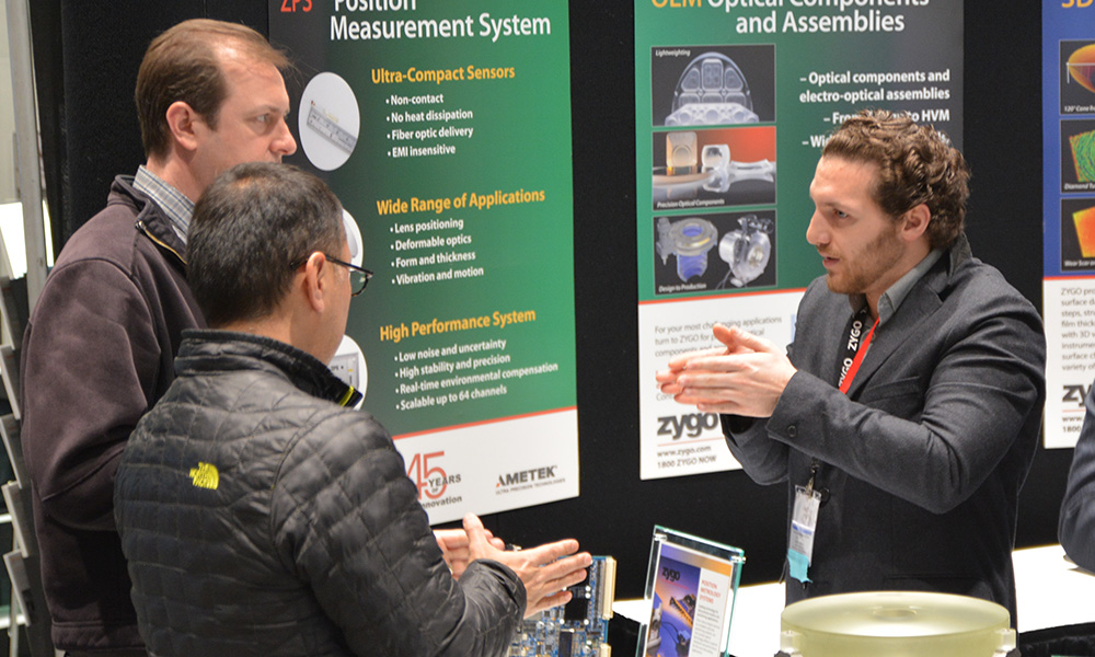
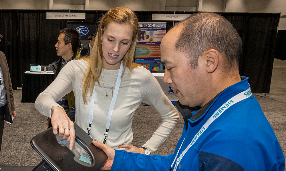
Exhibit in 2025 at SPIE Advanced Lithography + Patterning, Speakers discuss advanced lithography challenges and solutions at spie advanced lithography + patterning 2025. Spie advanced lithography + patterning:

SPIE Advanced Lithography Symposium Postscript Lithoguru, Spie advanced lithography + patterning: Spie advanced lithography + patterning is a conference and exhibition that addresses the challenges presented in optical and euv lithography, metrology, patterning.

Attend SPIE Advanced Lithography + Patterning, The event for emerging technology in the semiconductor industry. Access student opportunities, network with industry.
SPIE Advanced Lithography Conference Imec design papers SemiWiki, Join us for more learning opportunities in february 2025. Plan to attend the exhibition at spie advanced lithography + patterning to find the best solutions, components, instruments, and system providers from around the world.
SPIE Advanced Lithography Conference Imec design papers SemiWiki, Don't miss this opportunity to stay. Spie advanced lithography + patterning 2025.
Navigate to all elements of the spie advanced lithography + patterning program including conferences, courses, industry programming, networking opportunities, and special.